- Other Fluke companies:
- Fluke
- Fluke Biomedical
- Fluke Networks
- Fluke Process Instruments
Making Accurate DC Voltage Measurements in the Presence of Series Mode AC Signals
Authors: Paul Roberts and Martin Edwards. Fluke Precision Measurement Ltd.
1. Abstract
Accurate DC voltage measurements are not normally made in the presence of significant series
mode AC signals. Unwanted interference signals are avoided by use of appropriate lead and
guarding configurations, and other best measurement practices. However, there are some
applications where AC content is present – one example being the output of multijunction
thermal converters, where relatively high coupling between the heater and temperature sensing
elements results in a significant AC content on the DC output voltage. Another is measuring the
DC offset at the output of an AC source. This paper explores typical precision digital multimeter
(DMM) responses to and rejection of series AC mode signals, considers how their design
architecture influences the response, and suggests useful avoidance tactics to preserve
measurement accuracy.
2. Background
The DC Voltage function of a DMM is intended to measure signals that are essentially direct
voltages with minimal AC series (normal) mode content. Practically, some AC signal content or
pickup may be unavoidable and the DMM designs employ a number of features to remove or
reject the AC content and respond only to the average DC level. In precision applications large
amounts of AC signal would not usually be present, but there are cases where some AC content
is unavoidable and the DMM response, although minimal, might be significant in relation to the
required accuracy. One such case is where a nanovoltmeter is used to measure the output of a
multijunction thermal converter (MJTC), where relatively high coupling between the heater and
temperature sensing elements results in a significant AC content on the DC output voltage. A
recent international measurement comparison of ac-dc difference brought to light peculiar
problems experienced by several groups using planar MJTCs. Filipski and Boecker [1] also
investigated these problems and found that one particular kind of nanovoltmeter generated
significant frequency dependent common-mode errors. The observed effect was found to vary in
magnitude and sign with other nanovoltmeters of the same type. During a similar comparison,
Early [2] had found evidence of a similar normal mode effect introducing an apparent DC offset
using two different types of DMM, which lead to further investigation in co-operation with the
authors of this paper. (The relationship between common mode and normal mode effects is discussed later). To characterize the universality and significance of these offsets, further measurements are described using a number of common DMMs. With the recent release of a new precision 8.5 digit DMM, the Fluke 8508A, there was an opportunity to investigate the likely cause of these offset errors in the specific case of this DMM.
3. Dmm architecture and series mode response
Figure 1 shows a generalised block diagram for a typical DMM DC voltage function.

The signal scaling and conditioning circuits usually consist of attenuators and an input amplifier
which scale the input signal to an appropriate value for analog to digital conversion in the analog
to digital converter (ADC). Combinations of attenuation and gain provide the various ranges
available in the DMM. A low-pass filter may be included, either before or after the amplifier, to
remove unwanted AC signals and fast transients present on the DC input. The choice of
positioning the filter before or after the amplifier involves design tradeoffs such as low frequency
noise performance, allowable input dynamic range and circuit complexity.
Ideally a DC measuring instrument would respond only to the average value of its input signal,
in other words, to only the DC component of the input. The presence of AC components on the
DC input can have detrimental effects. Large AC signals in the input amplifier can cause it to
overload, and produce gross offsets. Typically bandwidth is relatively low, but smaller AC
signals can cause rectification problems in the active devices, especially at very high frequencies
as described in [3].
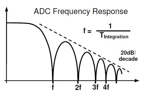
If AC signals are present in the ADC, they can cause ‘noisey’ readings. Typically, precision
DMMs use multislope integrating ADCs with integration times set to integral multiples of
power-line period to ensure that any line frequency related AC signal pickup is integrated out to
zero, and is therefore rejected. (The majority of unwanted AC pickup is usually from 50/60Hz
power-line sources). Appropriate choice of integration time can reject both 50Hz and 60Hz line
pickup. Figure 2 shows these ‘integration rejection notches’ in the ADC frequency response.
Other DMM designs may use a sample and hold circuit to acquire a sample of the signal for
conversion with some other form of analog to digital converter, which does not provide inherent
AC rejection. In this case the sample and hold sample time is typically set to multiples of line
period to provide line frequency AC rejection.
The foregoing considers series (normal) mode effects, caused by signals which appear
differentially between the DMM input terminals. Ideally a DMM should not respond to common
mode signals which appear equally on both the Hi and Lo input terminals with zero differential
content. In practice, the DMM circuitry (particularly the input amplifier) will have some
response to a common mode signal, effectively translating it into a series mode signal thorough
the imperfect common mode rejection of those circuits. The resulting series mode signal will be
diminished by a factor corresponding to the common mode rejection, and will stimulate any
series mode effects that may be present, albeit at a reduced level.
4. Observed Dmm series mode responses
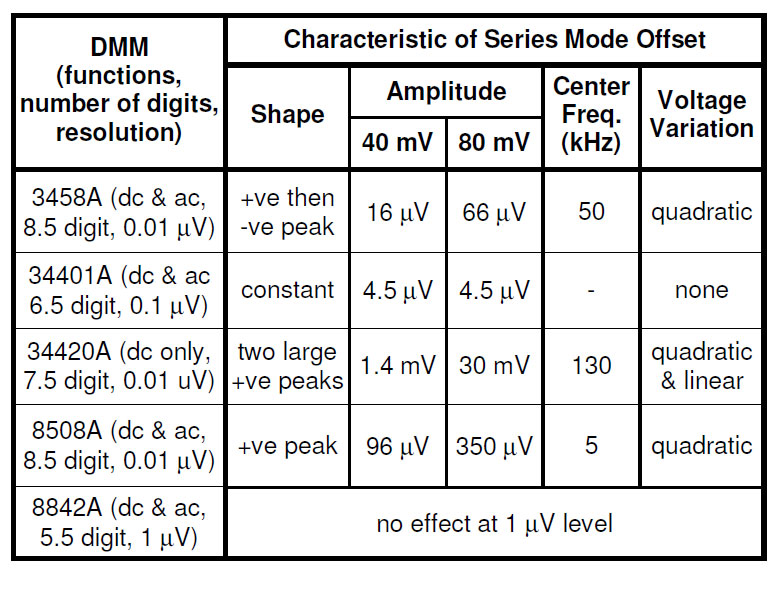
A summary of the measured offset behavior for a number of widely used DMM models is shown
in Table 1. A simple measurement circuit (refer to inset of Figure 3) consisting of an AC source
and a high pass filter to block any DC from the source is used to provide the series mode AC
voltage. The worst case DC offset observed on the DMM 100mV DCV (or equivalent) ranges is
recorded as a function of frequency for several values of applied RMS voltage.
for a range of DMMs identified by model number. All
DMM’s were set to the 100 mV DCV range (or similar)
and a 100 nF / 10 kΩ high pass filter was used.
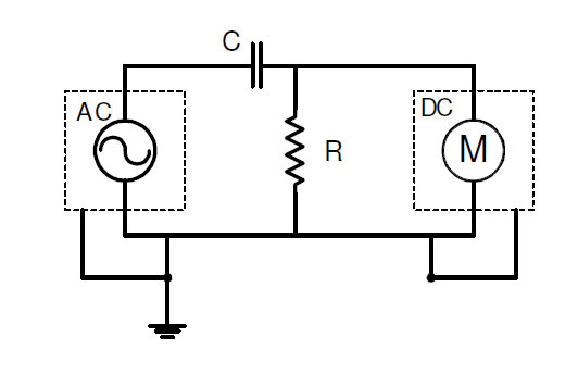
series mode offset. C and R form a high pass
filter blocking any DC offset from the AC
source.
The DMMs have significantly different circuit design architectures and the results show that the
pattern of offset behavior is similarly diverse. It is noteworthy that the lower precision 5.5 and
6.5 digit DMM appear to be immune to this particular effect.
5. Investigating the Fluke 8508A
The measured series mode response for the Fluke 8508A 8.5 digit DMM is shown in Figure 4,
demonstrating a peak at around 5kHz. A simplified block diagram for its DC voltage function is shown in Figure 5. The 8508A design reflects the intended metrology application, requiring precision at moderate reading rates rather than very high speed sampling (digitizing). R1 and C1 provide a low pass filter (-3dB at 10kHz) primarily to remove any fast transients on the input signal which may disturb or overload the preamplifier. The preamplifier scales the input signal prior to conversion in the multi-slope integrating analog to digital converter (ADC). In the 200mV range, the preamplifier has a gain of approximately 50. R2 and C2 provide low pass filtering to remove any fast transients prior to ADC conversion (-3dB at 40kHz), with additional filtering available from the selectable low pass filter. Not shown on this diagram are various protection and clamp circuits to prevent damage or malfunction in the event of overload or fault conditions. Initial investigations demonstrated that the offset is generated by the preamplifier itself, and is still present when the (non-linear) protection and clamp circuits are removed.
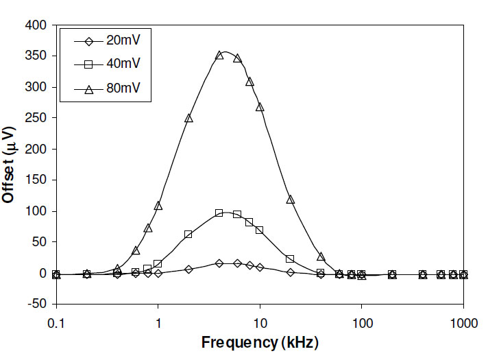
induced offset response. The legend shows the applied
RMS series mode voltage. Fig. 1 shows the circuit used to
make the measurements where C = 100 nF and R = 10 kΩ.
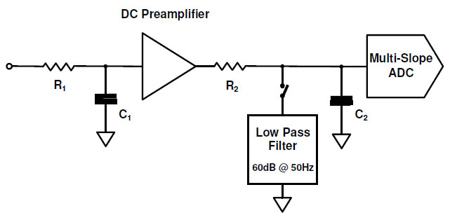
8508A DCV function.
The preamplifier is a discrete implementation of a non-inverting JFET input amplifier for the
main wideband signal path, with DC offset control from a parallel chopper stabilized low
frequency DC path. Figure 6 shows a block diagram of this topology.
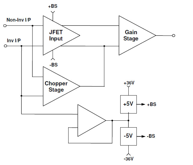
preamplifier stage of the Fluke 8508A. The chopper
operates at 20Hz, and crossover between the main
signal path and the chopper stabilized low frequency
path is 1Hz. Bootstrapping of the main signal path
input JFET stage provides adequate input common
mode range on the higher voltage ranges.
Detailed investigation has demonstrated the offset to be generated in the coupling between the
JFET input stage and the following gain stage. The peaking characteristic displayed in Figure 4
is due to the crossover between the inherent series mode offset effect within the preamplifier
which increases in magnitude with increasing frequency and the low-pass filter formed by R1 and
C1 which attenuates the series mode signal ahead of the preamplifier. The gain bandwidth
product of the preamplifier also has an impact. The 200mV range is the highest gain
configuration, and demonstrates the most significant susceptibility to this particular effect. On
the higher ranges, where the preamplifier gain is reduced, the amount of offset appearing is
proportionally much less.
5. Application guidance and avoidance tactics
Use of appropriate lead and guarding configurations, and other best measurement practices will
avoid most unwanted interference signals. For example, the use of twisted pair leads, shielded
leads etc to minimise pick-up of AC signals when making precision DC or resistance
measurements. Large AC signals can overload the input stages of a DMM DC function and
generate gross offset effects. If a significant AC component on the DC signal is unavoidable,
applying an external low-pass filter prior to the DMM input can be helpful.
One example is the measurement of the DC offset present at the output of an AC signal source.
In this case, the AC signal can be very large in comparison to the DC level to be measured. The
filter should be chosen to give sufficient attenuation of the AC signal, but avoid excessive series
resistance which might introduce an effective offset with the DMM input bias current flowing.
Typical precision DMM input current is usually in the region of a few picoamps or tens of
picoamps (lower precision DMMs can have much higher input currents). A simple Ohm’s Law
calculation will give an indication of likely bias current induced offset effect. Alternatively, use
the DMM offset null or input zero feature to zero out any offset, taking care to apply the short
circuit ahead of the filter. Excessive additional series resistance can also introduce noise (caused
by the inherent thermal noise generated in any resistance), which might be significant in some
applications. The circuit being measured may be sensitive to any impedance connected to it,
bearing in mind that the input impedance of the DMM will be modified by any filter circuit
added externally to the DMM. Ensure component ratings are adequate for the applied voltages.
Some DMM designs incorporate an internal user-selectable low-pass filter, but users should be
aware that in some DMM designs the filter may be placed after the input amplifier, so may not
eliminate effects generated within the DMM input amplifier itself.
It is difficult to generalise, but in the case of the 8508A, a simple RC low-pass filter added at the
terminals will be effective in most applications for minimising the series mode susceptibility
discussed in this paper. See Figure 7 for filter details. At 15kΩ the resistor is chosen to avoid
adding significant amounts of noise, and adds <0.75μV offset at the specified <50pA bias current
for the 8508A. With a 220nF capacitor the filter 3dB corner frequency is at approximately 60Hz,
providing 40dB of series mode AC signal attenuation at 5kHz where the 8508A is most sensitive
to the series mode effect described, reducing the effect by 100 times. Other filter designs might be more appropriate for different measurement situations, depending on the circuit configuration
and signals present.
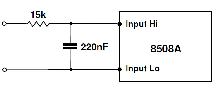
DMM DCV function to minimise its series
mode offset effect. Ensure component ratings
are adequate for the voltages applied.
If measurements are being made on the most sensitive range, another approach is to use a higher
range and take advantage of the diminished susceptibility due to preamplifier gain reduction on
higher ranges. For example with the 8508A, changing up to the 2V range from the 200mV range
dramatically reduces susceptibility, but with 8.5digit resolution available, sufficient precision for
most applications can be maintained.
6. Conclusions
High precision DMMs can be susceptible to normal mode offsets, but for the majority of
applications requiring precision DC voltage measurement these effects are not significant. If AC
series mode signals are present users should be aware of their impact and the possibility that
spurious offsets may be present. However, using good measurement practice to avoid AC signal
pickup, or the using filters to remove unavoidable AC signals will eliminate series mode offsets
in most applications.
7. References
- P. S. Filipski and M. Boecker, “Experience with High-Output-Resistance MJTC AC-DC
Transfer Standards at High Frequencies”, IEEE Trans. Instrum. Meas., Vol. IM-52, No. 4, pp.
1314-1319, August 2003. - P. C. A. Roberts and M. D. Early “Normal Mode Offsets in High Performance Digital
Multimeters”, CPEM Conference, June 2004. - F. Fiori, “Integrated Circuit Susceptibility to Conducted RF Interference”, Compliance
Engineering Magazine., Nov/Dec 2000. (https://www.cemag.
com/archive/2000/novdec/fiori.html)
- Home
- Products
- New Products
- Electrical Calibration
- RF Calibration
- Data Acquisition and Test Equipment
- Temperature Calibration
- Humidity Calibration
- Pressure Calibration
- Flow Calibration
- Process Calibration Tools
- Calibration Software
- Service and Support
- All Calibration Instruments
- Purchase Info
- News
- Training and Events
- Literature and Education
- Service and Support
- About Us

